What Is GaN Technology? A Manufacturer's Guide for Power Adapter Buyers
Lisa, a product manager at a Rotterdam-based IoT brand, stared at the mechanical drawing for her new gateway. The enclosure was 30% smaller than the previous generation, but the 65W adapter her team had specified was not. She needed the same power in a smaller volume, and she needed it without the charger running hot enough to derate the housing. That is the exact problem GaN technology was built to solve.
If you source AC/DC power adapters or chargers for consumer electronics, e-mobility, or IoT devices, you have probably seen "GaN" on adapter labels and datasheets. It is more than a marketing badge. Gallium nitride is a different semiconductor material that changes how switching power supplies convert AC wall power into stable DC output. In this guide, we will explain what GaN technology is, how it works, where it outperforms silicon, and what you should verify before specifying a GaN adapter for your next product.
Want to see how GaN adapters fit your enclosure and efficiency targets? Browse our AC/DC power adapter range or request a free sample with current test reports.
What Is GaN Technology?
GaN stands for gallium nitride, a compound semiconductor made from gallium and nitrogen. Unlike the silicon that has dominated power electronics for decades, GaN is a wide bandgap material. That means the energy gap between its valence band and conduction band is wider than silicon's. The practical result is that GaN devices can switch faster, handle higher voltages, and waste less energy as heat.
In a switching power supply, the transistor inside the adapter turns on and off thousands of times per second to chop the incoming AC waveform into a high-frequency pulse train. That pulse train is then filtered into smooth DC.
Silicon transistors have done this job well for years, but they reach physical limits at higher frequencies and voltages. GaN transistors break through those limits. They can switch at higher frequencies with lower switching losses, which lets designers use smaller transformers, smaller capacitors, and smaller enclosures without sacrificing output power.
This is why a 65W GaN adapter can be roughly half the size and weight of a 65W silicon adapter. The material itself is not smaller; the magnetics and passive components around it are.
How GaN Technology Works in a Power Adapter
To understand GaN technology, it helps to look at the three places it changes adapter design.
Higher Switching Frequency
A typical silicon-based flyback converter switches at 50–100 kHz. A GaN-based design can switch at 200 kHz, 500 kHz, or even higher. Higher frequency means each energy pulse is smaller, so the transformer and inductor can be smaller for the same power throughput. The transformer is usually the largest component in an adapter, so shrinking it directly shrinks the whole unit.
Lower Switching Losses
Every time a transistor switches, a small amount of energy is lost in the transition. Silicon transistors lose more energy during these transitions, especially at high frequency. GaN devices have lower gate charge and faster rise/fall times, so they lose less energy per switch. Therefore, lower losses mean higher efficiency and less heat.
Lower On-Resistance
GaN devices can achieve lower on-resistance for a given breakdown voltage than silicon MOSFETs. Lower on-resistance means less conduction loss when the transistor is fully on. That translates to higher full-load efficiency, which is exactly what standards like DOE Level VI measure.
The combination of these three effects is what makes GaN technology attractive for compact, high-power-density adapters.
GaN vs Silicon: A Side-by-Side Comparison
When procurement engineers evaluate GaN adapters, they usually want a direct comparison against the silicon platform they already use. Here is how the two materials stack up in real adapter applications.
| Attribute | Silicon (MOSFET) | GaN (Gallium Nitride) |
|---|---|---|
| Bandgap | 1.1 eV | 3.4 eV |
| Typical switching frequency | 50–100 kHz | 200 kHz–1 MHz+ |
| Switching losses | Higher | Lower |
| On-resistance at high voltage | Higher | Lower |
| Efficiency at full load | Good | Better (often 1–3% higher) |
| Operating temperature | Higher for same loss | Lower for same loss |
| Power density | Lower | Higher (smaller size for same W) |
| Component count | Standard | Reduced magnetics/passives |
| Cost per device | Lower | Higher (but gap is narrowing) |
| Maturity | Very mature | Mature for adapters under 240W |
The efficiency difference sounds modest, but it compounds. A 65W adapter that moves from 90% to 92% efficiency wastes 1.3W less as heat. That is enough to eliminate a fan, reduce enclosure size, or extend the ambient temperature rating.
Marcus, a buyer for a Berlin e-bike brand, learned this the hard way. His first-generation 84V charger used a silicon platform. It worked, but the enclosure had to be oversized to handle the thermal rise during a 4-hour charge cycle.
When his engineering team switched to a GaN-based primary stage for the second generation, the operating temperature dropped by 12°C. The smaller enclosure saved freight cost, and the lower case temperature became a selling point for end users.
Why GaN Technology Matters for OEM Buyers
For brand owners and procurement engineers, GaN technology is not just a semiconductor curiosity. It changes four things that directly affect product design, cost, and customer experience.
Smaller Product Envelopes
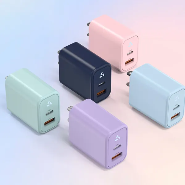
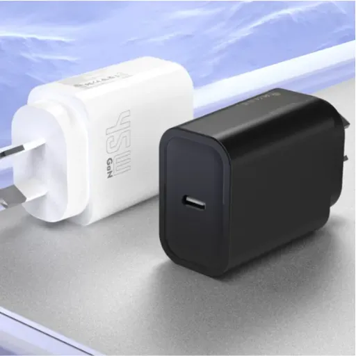
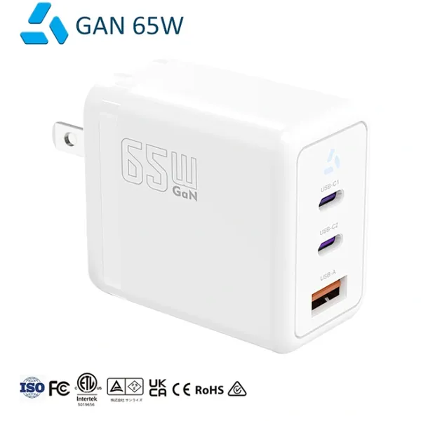
GaN lets you deliver the same wattage in a smaller adapter. That matters when your product has a tight enclosure, when retail shelf space is limited, or when end users carry the adapter in a bag. A 65W GaN USB-C adapter can be roughly the size of a traditional 30W silicon adapter.
Higher Energy Efficiency
GaN adapters typically score higher on active-mode efficiency tests. GaN charger efficiency is most visible at 50–100% load, which is why the technology pairs well with USB-C PD and high-power adapters. That helps with DOE Level VI compliance, EU ErP Tier V, and ENERGY STAR Level V requirements. It also means lower energy bills for end users and less thermal stress on the product.
Reduced Thermal Design Risk
Less waste heat means smaller heat sinks, less airflow dependency, and wider operating temperature range. Consequently, outdoor applications like security cameras, LED drivers, or IoT gateways gain valuable thermal headroom.
Improved Power Density for High-Wattage Chargers
As chargers push past 100W for laptops, tablets, and power tools, silicon designs become bulky. GaN technology keeps these adapters portable. It is also moving into higher-power applications like server power supplies and on-board EV chargers, though consumer adapters remain the most mature market.
Ready to test the difference in your own product? Request a GaN adapter sample and compare size, temperature, and efficiency against your current silicon platform.
Common Applications of GaN Technology
GaN technology is already mainstream in several product categories. If you are specifying power products, you will encounter it most often in these areas.
Consumer Electronics Adapters
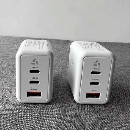
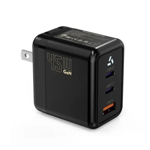
Smartphone and laptop chargers were the first mass-market gallium nitride power adapter applications. A 65W or 100W USB-C adapter that fits in a pocket is now normal thanks to GaN. These adapters also tend to have multi-output ports, which adds value for travelers and multi-device users.
USB-C PD Chargers
USB Power Delivery (PD) profiles from 18W to 240W rely on precise voltage negotiation and high-frequency conversion. GaN's fast switching pairs well with the dynamic load changes of USB-C PD. This is why most premium GaN adapters target PD applications.
Compact AC/DC Adapters for IoT
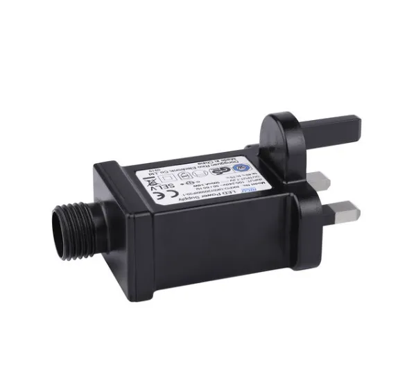
Routers, gateways, smart home hubs, and security panels often live in tight enclosures or behind furniture. A GaN adapter delivers the required 12V, 24V, or 48V output without the bulk of a traditional brick. Lower heat also helps when the adapter is enclosed or wall-mounted.
Outdoor and Industrial Power Supplies
IP65 or IP67 outdoor adapters benefit from GaN because the sealed enclosure traps heat. Lower losses mean the internal temperature stays further from component limits. That improves long-term reliability in sun-exposed or industrial environments.
Emerging High-Power Applications
GaN is moving into data center power supplies, telecom rectifiers, and automotive on-board chargers. These applications demand very high efficiency and power density. While consumer adapters are the most proven market today, the technology roadmap points upward in power.
GaN Technology Limitations and Misconceptions
However, GaN is not a universal replacement for silicon. Smart buyers understand the trade-offs.
Cost Is Still Higher
GaN devices cost more than silicon MOSFETs at the component level. The gap has narrowed significantly, and the savings in magnetics, enclosure, and freight often offset the device premium. Still, for very cost-sensitive, low-power adapters, silicon can remain the better choice.
Layout and EMI Are More Demanding
GaN switches so fast that printed circuit board layout becomes critical. Poor layout can cause ringing, electromagnetic interference (EMI), and reliability issues. This means GaN designs require more experienced power-electronics engineering and more careful EMI filtering than silicon equivalents.
Not All GaN Adapters Are Equal
Putting a GaN transistor into a silicon-designed circuit does not automatically produce a great adapter. The controller, gate driver, transformer, snubber network, and EMI filter all need to be optimized for GaN. A poorly designed GaN adapter can be less efficient and less reliable than a well-designed silicon one.
Efficiency Gains Vary by Load
GaN shines brightest at moderate-to-high loads and high switching frequencies. At very light loads, a well-designed silicon adapter may still be competitive. Always request efficiency curves across 25%, 50%, 75%, and 100% load before making a decision.
How to Specify a GaN Adapter for Your Product: OEM Buyer Checklist
If you are considering GaN for your next adapter or charger, treat it like any other power supply qualification. For a GaN adapter OEM project, verify the specifications that affect real-world performance and certification.
1. Define Output Voltage, Current, and Power
Start with your product's input requirements. A 65W USB-C PD adapter and a 24V 2.5A industrial adapter are both GaN candidates, but the designs are very different. Lock down voltage, current, ripple, and transient response before talking to suppliers.
2. Request Efficiency Curves at All Load Points
Do not settle for a single efficiency number. Ask for efficiency at 25%, 50%, 75%, and 100% load, plus no-load power. Compare these against DOE Level VI or ErP Tier V limits for your target market. The curve tells you far more than a headline number.
3. Verify Thermal Performance
Ask for operating temperature rise data at full load in a realistic ambient temperature. A GaN adapter should run cooler than a silicon equivalent at the same wattage. If it does not, the design may not be fully optimized.
4. Confirm Certification Stack
GaN does not exempt an adapter from safety and efficiency certifications. Verify the same marks you would require for silicon: UL, CE, UKCA, FCC, SAA, CB, and DOE Level VI or ErP Tier V as applicable. Request current test reports with traceable report numbers.
5. Evaluate EMI Test Reports
Because GaN switches faster, EMI compliance can be challenging. Make sure the supplier provides conducted and radiated EMI test data, typically to EN 55032 or FCC Part 15 Class B. This is especially important for adapters feeding sensitive electronics.
6. Plan for Connector and Cable Compatibility
Smaller adapters sometimes use custom connectors or shorter cables to save space. Confirm that the connector, cable length, and strain relief match your product's assembly and end-user expectations.
7. Understand the BOM and Supply Chain
Ask which GaN device the supplier uses and whether it is a second-sourced platform. GaN semiconductor availability has improved, but supply-chain transparency still matters for long-term production planning.
Sofia, a sourcing manager for a Dubai security brand, ran through this checklist for a new outdoor camera line. Her team initially selected the smallest adapter on the market, but the supplier could not produce a current EMI report. They switched to a slightly larger GaN design with full UL, FCC, and IP67 documentation. The product launched on time, and customs clearance in Jebel Ali went smoothly because the paperwork matched the unit.
GaN Technology and the Future of Power Supplies
The shift from silicon to GaN is not a fad. It is a materials transition that mirrors the earlier move from bipolar transistors to MOSFETs. As GaN device costs fall and device portfolios expand, the technology will move into higher wattages and more applications.
For OEM buyers, the strategic question is not whether GaN is real. It is whether GaN fits your specific product, volume, and cost structure.
In many cases, the answer is yes. The smaller size, lower heat, and higher efficiency help products stand out in competitive markets. In other cases, a mature silicon design may still deliver the best total cost of ownership.
The best approach is to qualify both options for your next design. Run samples side by side, measure temperature and efficiency in your actual enclosure, and compare the landed cost including enclosure, freight, and certification. That data will tell you which platform wins for your application.
Conclusion
GaN technology has moved from laboratory curiosity to production reality in consumer and industrial power supplies. It lets manufacturers build smaller, cooler, and more efficient adapters by replacing silicon transistors with gallium nitride devices that switch faster and waste less energy.
Here are the key takeaways for OEM buyers:
GaN is a wide bandgap semiconductor that enables higher switching frequency and lower losses than silicon.
GaN adapters are typically smaller, lighter, and more efficient than silicon equivalents at the same power level.
The technology is mature for consumer adapters, USB-C PD chargers, and compact IoT power supplies.
Cost, EMI design, and layout are more demanding with GaN, so supplier engineering capability matters.
Always request efficiency curves, thermal data, EMI reports, and current certification documents before qualifying a GaN adapter.
If you are sourcing AC/DC adapters or chargers and want to explore whether GaN technology fits your next product, the next step is simple. Send us your voltage, current, and enclosure requirements. Our engineering team will propose a GaN or silicon platform based on your actual specification and share efficiency curves and sample timelines within 24 hours.
Get an OEM quote for your GaN adapter or request a free sample to compare size, temperature, and efficiency against your current design.
Recently Posted
-
GaN Charger vs Normal Charger: An OEM Buyer's Comparison
June 12, 2026Last spring, a product manager at a Berlin laptop accessory brand opened two 65W samples on his desk. One was a normal silicon cha Read More
 -
What Is a GaN Charger? A Buyer’s Guide to Gallium Nitride Power Adapters
June 12, 2026In 2024, Maria Chen’s team at a Shenzhen router OEM received a blunt message from their largest U.S. distributor: shrink the power Read More
 -
What Is Power Delivery? Understanding Energy Transfer in Modern Electronics
June 12, 2026When Ravi Patel, a hardware engineer at a consumer electronics firm in Mumbai, received the first production samples of his team&# Read More
 -
USB C Charging Wattage: What OEM Buyers Need to Know Before Specifying a PD Adapter
June 12, 2026A 65W USB-C charger and a 65W USB-C charger are not the same thing. Same number on the label. Entirely different behavior in the f Read More

Contact Us
Recommended Products
-
 65W USB-C GaN Wall Charger PD Fast Charging Adapter EU US Plug for Laptop Smartphone and TravelUS$ 6MOQ: 100 Pieces
 -
45W GaN USB-C Fast Charger JP Plug PD Wall Charging Adapter for IPhone MacBook and TabletsUS$ 8MOQ: 100 Pieces
-
QC3.0 30W USB Fast Charger With 18W Quick Charge Wall Adapter for Android and Mobile DevicesUS$ 4MOQ: 100 Pieces
-
Compact 18W Quick Charge 3.0 USB Charger 30W Fast Charging Adapter EU US Plug for TravelUS$ 2MOQ: 100 Pieces
-
30W USB-C and USB-A PD Fast Charger Compact Wall Adapter for IPhone Samsung and IPadUS$ 3MOQ: 100 Pieces
-
35W Dual USB-C PD Charger Fast Charging Adapter for IPhone Samsung IPad and USB-C DevicesUS$ 3MOQ: 100 Pieces
-
65W USB-C GaN Charger EU Plug Fast Charging Adapter 65W USB-C PD Fast Charge Wall Charger Power Adapter for Macbook ProUS$ 5MOQ: 100 Pieces
-
65W GaN USB-C Fast Charger PD Wall Charging Adapter for Laptop IPhone and Mobile DevicesUS$ 5MOQ: 100 Pieces
-
100W GaN USB-C Fast Charger With PD 3.0 for Laptop, MacBook, IPhone & Multi-Device ChargingUS$ 12MOQ: 100 Pieces
-
45W GaN USB-C Fast Charger EU AU PD Fast Wall Charging Adapter for IPhone Tablets With CE REACH PassedUS$ 8MOQ: 100 Pieces
-
QC3.0 65W GaN USB C Super Fast Charger With UKCA 3 Ports PD 3.0 GaN Charger for Iphone Macbook SamsungUS$ 10MOQ: 100 Pieces
-
30W USB-C and USB-A GaN QC3.0 Fast Charging Adapter PD Fast Charger Compact Wall Adapter for IPhone Samsung and IPadUS$ 3MOQ: 100 Pieces
-
45W GaN USB-C Fast Charger With Dual Type-C and USB-A Ports PD Wall Charging AdapterUS$ 8MOQ: 100 Pieces
-
Dual USB C Ports QC3.0 30W Fast Charger With EU UK AU US USB-C PD Wall Chargeer 30W PD Power AdapterUS$ 3MOQ: 100 Pieces
-
Compact 65W GaN USB-C Wall Charger With Dual USB-C Ports and USB-A Fast Charging Adapter With CE UKCA ETL SAAUS$ 10MOQ: 100 Pieces
-
QC3.0 Fast Charging Adapter PD30W USB-C USB-A GaN PD Fast Charger PD 3.0 GaN Charger Compact Wall Adapter for IPhone Samsung and IPadUS$ 3MOQ: 100 Pieces
-
12V 5A 60W US EU AC DC Adapter LED Driver LED SMPS AC to DC Switching Power SupplyUS$ 5 - 7MOQ: 50 Pieces
-
CE FCC CUL SAA KC PSE 24Vdc 48W Switching Power Supply AdaptersUS$ 5 - 7MOQ: 50 Pieces
-
CE GS UKCA SAA CUL Qualified Waterproof Switching Power Supply Ip68 PSE UL SAA GS 12V 2AUS$ 3 - 6MOQ: 50 Pieces
-
12V 1A Factory OEM Waterproof AC Adapter for Laser Light Table Lamp ac dc Adaptor With TUV CE GS for EU MarketUS$ 5 - 7MOQ: 50 Pieces