GaN Charger vs Regular Charger: What OEM Buyers Need to Know Before Specifying
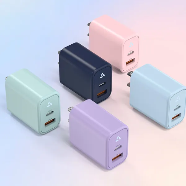
A 65W GaN charger is roughly 40% smaller than its silicon equivalent, yet it runs cooler, wastes less energy, and handles the same load. For OEM buyers shipping millions of units annually, that size difference changes packaging dimensions, freight costs, and shelf appeal — all while the end user gets a cooler, more efficient adapter.
If you're deciding whether to specify a gallium nitride (GaN) charger or a traditional silicon-based charger for your next product line, this guide gives you the engineering comparison that matters. You'll learn how GaN technology changes power density, thermal behavior, efficiency curves, and unit cost. You'll also see exactly which applications benefit most from GaN, and where silicon still makes sense. Every claim is backed by measurable specs, not marketing slogans.
At Anenerge, we've built both GaN and silicon AC/DC adapters across our three Panasonic SMT lines. This article draws on actual production data, thermal test results, and the field-failure analysis we run in our in-house laboratory.
Want to see the size difference for yourself? Request a free GaN sample and a matching silicon equivalent — we ship engineering samples within 7 days so you can compare them side by side in your enclosure.
What GaN Technology Actually Changes
GaN stands for gallium nitride, a wide-bandgap semiconductor material. In plain terms, that means electrons can move through GaN faster than through silicon, and GaN can switch at higher frequencies with lower energy loss.
For charger design, three properties matter most:
Higher switching frequency: GaN transistors switch at 500 kHz to 2 MHz, compared to 50–100 kHz for silicon MOSFETs. Higher frequency means smaller magnetics — the transformer and inductor shrink.
Lower on-resistance: GaN devices have lower resistance when conducting, which reduces conduction losses and heat generation.
Lower gate charge: GaN switches faster with less driving energy, improving efficiency at light loads.
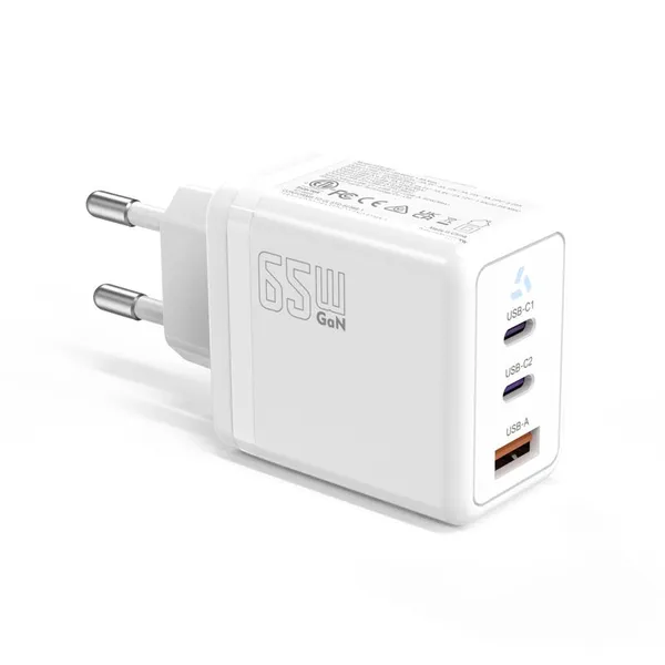
What does this mean for the physical adapter? A 65W GaN charger typically measures 50 mm × 50 mm × 30 mm. A 65W silicon charger with equivalent output is closer to 65 mm × 65 mm × 35 mm. The volume reduction is approximately 40–50%. The weight drops by a similar margin.
Engineering note: GaN doesn't eliminate the need for good thermal design. It reduces heat generation, but the smaller enclosure has less surface area to dissipate what remains. A well-designed GaN charger pairs the semiconductor advantage with careful enclosure engineering.
The shift from silicon to GaN isn't theoretical. Apple, Samsung, Anker, and Baseus have all moved their flagship multi-port chargers to GaN. For OEM buyers, the question is no longer whether GaN works — it's whether GaN fits your application, volume, and cost target.
Size, Weight, and Power Density: The Numbers That Matter
Power density — watts per cubic centimeter — is where GaN separates from silicon. Here is how the numbers compare at common wattages:
| Wattage | GaN Power Density | Silicon Power Density | Size Reduction |
|---|---|---|---|
| 30W | ~0.9 W/cm³ | ~0.4 W/cm³ | ~55% |
| 45W | ~1.0 W/cm³ | ~0.5 W/cm³ | ~50% |
| 65W | ~1.2 W/cm³ | ~0.6 W/cm³ | ~50% |
| 100W | ~1.4 W/cm³ | ~0.7 W/cm³ | ~50% |
| 140W | ~1.5 W/cm³ | ~0.8 W/cm³ | ~47% |
These figures are approximate and vary by design, but the pattern is consistent. GaN delivers roughly double the power density of silicon across the 30W–140W range.
When Maria, a product manager at a Berlin-based e-bike brand, switched her 48V accessory adapter from a 60W silicon design to a 60W GaN platform, the carton dimensions shrank by 38%. On a 10,000-unit sea-freight shipment from Shenzhen to Hamburg, that translated to roughly 12 fewer cubic meters of cargo space. At her forwarder's rate, the freight savings alone paid for the GaN unit cost premium within two production runs.
For brand owners, smaller chargers also mean:
Smaller retail packaging: Less cardboard, less shelf space, lower packaging cost
Lower shipping weight: Air freight savings add up at volume
Improved user experience: End users prefer compact adapters, especially for travel and portable electronics
More interior space: In products where the adapter is built in (desktop monitors, all-in-one PCs), smaller power boards free enclosure space for other components
Thermal Performance and Reliability in Real Applications
Smaller size raises a natural question: does GaN run hotter? The answer depends on design quality, but well-designed GaN chargers typically run cooler than silicon equivalents at the same wattage.
The reason is efficiency. A GaN charger loses less energy as heat during the switching process. Even though the enclosure is smaller, the total heat generated is lower.
At Anenerge, our 65W GaN adapters measure approximately 42°C surface temperature at full load in a 25°C ambient environment. Comparable silicon designs at the same load and ambient run closer to 52–58°C.
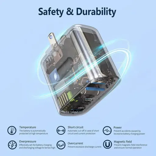
However, thermal management isn't automatic. GaN's high switching frequency can create more electromagnetic interference (EMI) if the PCB layout is poor. The smaller enclosure leaves less room for heat sinks. And GaN devices are more sensitive to over-voltage stress on the gate — a design flaw that wouldn't harm silicon can destroy a GaN transistor.
That's why supplier selection matters. A generic Shenzhen factory that simply swaps a silicon MOSFET for a GaN transistor without redesigning the PCB, magnetics, and EMI filter will produce a charger that runs hot, fails EMI, and dies young. A proper GaN design requires:
Optimized PCB layout for high-frequency switching
Smaller, higher-frequency magnetics (planar transformers, integrated inductors)
Careful gate drive design to protect the GaN device
Revised EMI filtering for the higher switching frequency
Thermal simulation and validation in the target enclosure
At Anenerge, every GaN design goes through the same validation process as our silicon platforms. We run thermal imaging at 25°C, 40°C, and 50°C ambient. We do full-load burn-in for 4 hours. Then we run EMI pre-scan in our lab before third-party certification submission.
Efficiency and Energy Standards Compliance
GaN chargers typically achieve 1–3% higher efficiency than silicon equivalents at the same wattage. That sounds small until you multiply it across production volume.
Consider a 65W adapter running at 50% load (typical for a laptop charger):
Silicon: ~90% efficiency → 6.5W lost as heat
GaN: ~93% efficiency → 4.55W lost as heat
The difference is 1.95W per adapter. Across 100,000 units running 8 hours per day, 250 days per year, that is 390,000 kWh saved annually. At $0.12 per kWh, the energy savings exceed $46,000 per year — on a single SKU.
For regulatory compliance, the efficiency advantage matters too:
DOE Level VI: The U.S. standard requires specific minimum efficiency based on rated output. GaN makes it easier to hit the mark with margin, especially at lower wattages where the standard is tight relative to silicon capability.
ENERGY STAR Level V: More demanding than DOE Level VI. GaN's light-load efficiency advantage helps here, where many silicon designs struggle.
ErP Tier V: The European equivalent. GaN adapters comfortably exceed Tier V requirements across the load range.
Brands selling into regulated markets — the U.S., EU, UK, Australia — benefit from GaN's efficiency headroom. It provides a safety margin against production variability and ensures compliance even as components age. Learn more about what DOE Level VI requires in our DOE Level VI compliance guide.
Cost Analysis: BOM, Unit Price, and Total Cost of Ownership
GaN semiconductors cost more than silicon MOSFETs. At the component level, a GaN power IC costs roughly 2–3x its silicon equivalent. But the system-level cost picture is more nuanced.
Here is a typical BOM cost breakdown for a 65W USB-C charger at 10,000-unit volume:
| Cost Component | Silicon | GaN | Delta |
|---|---|---|---|
| Power transistor | $0.80 | $2.40 | +$1.60 |
| Transformer | $1.20 | $0.90 | -$0.30 |
| Inductor / filter | $0.60 | $0.40 | -$0.20 |
| Heat sink | $0.40 | $0.15 | -$0.25 |
| Enclosure | $0.80 | $0.60 | -$0.20 |
| PCB area | $0.50 | $0.40 | -$0.10 |
| Total BOM | ~$4.30 | ~$5.05 | +$0.75 |
The GaN BOM is roughly $0.75 higher at 65W. At 10,000 units, that is $7,500. But the savings in magnetics, heat sinking, enclosure material, and PCB area partially offset the semiconductor premium.
Total cost of ownership tells a different story. Factor in:
Freight savings: Smaller, lighter cartons reduce shipping cost
Packaging savings: Smaller retail boxes use less material
Energy savings: Higher efficiency reduces end-user electricity cost (relevant for sustainability claims)
Shelf appeal: Compact chargers command higher retail prices in consumer channels
Thermal reliability: Cooler operation can extend product life and reduce warranty returns
When the procurement team at a Dutch IoT gateway manufacturer modeled the full cost, the GaN adapter's $0.80 unit premium was recovered within the first production run through freight and packaging savings alone. By the third run, the GaN platform was cheaper on a total-cost basis.
For OEM buyers, the question isn't "is GaN more expensive?" — it's "where does GaN pay back, and on what timeline?" For high-volume, shipping-intensive, or consumer-facing products, the payback is often immediate. For low-volume industrial applications with loose size constraints, silicon may still be the rational choice.
When to Specify GaN vs. Silicon for Your Product Line
GaN isn't the right choice for every application. Here's how to decide based on real product requirements.
Specify GaN when:
Size and weight matter: Travel adapters, compact laptop chargers, wall-mount adapters where the plug body must be small
Thermal constraints are tight: Adapters built into enclosures with limited airflow (monitors, all-in-one PCs, IoT gateways)
Efficiency margins are critical: Products targeting ENERGY STAR, DOE Level VI, or ErP Tier V with minimal headroom
Multi-port output is needed: GaN's efficiency at light loads makes it ideal for chargers with 2–4 ports where single-port load varies
Premium positioning: Consumer brands where compact size is a selling feature
High power density required: Adapters above 65W where silicon becomes bulky
Stick with silicon when:
Cost is the primary driver: Ultra-cost-sensitive products where every cent of BOM matters
Size is not constrained: Desktop adapters, industrial enclosed power supplies with generous mounting space
Power levels are low: Below 30W, the size and efficiency advantage of GaN diminishes relative to the cost premium
Mature, proven design is preferred: Long-life industrial products where design stability outweighs incremental improvement
** EMI sensitivity is extreme**: Some medical and measurement instruments require conservative EMI design where silicon's lower switching frequency is an advantage
James, a procurement engineer at a U.S. security camera manufacturer, learned this the hard way. He specified GaN for a 12V 2A wall adapter without checking the enclosure first. The camera's junction box had just 30 mm of internal depth. The GaN adapter fit, but the reduced heat-sinking surface area caused the internal temperature to climb 8°C above the silicon equivalent in summer conditions.
For his next revision, he returned to silicon. Not because GaN failed, but because the enclosure was designed for silicon's thermal profile.
The lesson: match the technology to the application, not the trend.
Sourcing GaN Chargers: What to Verify From Your Supplier
Not every factory claiming "GaN technology" delivers a genuine GaN benefit. Some suppliers use GaN transistors in poorly optimized designs that run hot, fail EMI, or cost more than they should. Here is what to verify before placing a production order.
1. Verify the GaN Device Manufacturer
Quality GaN power ICs come from established suppliers: Navitas, GaN Systems (now Infineon), Power Integrations (InnoSwitch), Texas Instruments, and ON Semiconductor. Ask your charger supplier which GaN device they use. If they can't name the IC or provide a datasheet, that's a red flag.
2. Request Thermal Test Data
Ask for surface temperature measurements at:
25°C ambient, 100% load, continuous operation
40°C ambient (simulating a warm office or enclosed space)
After 4-hour burn-in
The data should include thermal images, not just single-point thermometer readings. A well-designed GaN charger should run cooler than a silicon equivalent at the same wattage and ambient temperature.
3. Check Efficiency Curves at Multiple Load Points
DOE Level VI tests at 25%, 50%, 75%, and 100% load. Request the efficiency curve across this range. GaN's biggest advantage is often at light load (25–50%), where silicon designs struggle. If the GaN charger only beats silicon at 100% load, the design is not optimized.
4. Confirm EMI Pre-Scan Results
High-frequency switching can produce more EMI if the layout is poor. Ask for conducted EMI scan results against EN 55032 / CISPR 32 limits. The GaN charger should pass with margin, just like a silicon design.
5. Review the Certification Stack
GaN doesn't change the certification requirements. The adapter still needs:
U.S.: UL 62368-1, FCC Part 15, DOE Level VI
EU: CE (EN 62368-1, EN 55032/35), ErP Tier V
UK: UKCA
Australia: SAA / RCM
Verify the supplier has current test reports for the exact GaN model you plan to order. Don't accept a silicon adapter's certifications as proof for a GaN variant — the design is different and needs its own test reports.
6. Validate the Charge Profile (for Battery Chargers)
If you are sourcing a GaN battery charger rather than an AC/DC adapter, verify the CC-CV profile is tuned to your cell chemistry. GaN enables higher power density, but the charge curve must still match your pack's requirements. Browse our LiFePO4 battery charger range to see how chemistry-matched charging works across different platforms.
7. Ask About Production Volume and MOQ
GaN designs often require slightly higher MOQs than silicon because the GaN IC supply chain is tighter and the PCB assembly process is more sensitive. At Anenerge, our standard GaN adapter MOQ starts at 1,000 units for OEM-customized designs. Standard catalog GaN SKUs start at 500 units.
Ready to compare GaN and silicon for your application? Contact our engineering team with your voltage, current, and enclosure requirements. We will recommend the right platform and ship a matched pair of samples within 7 days.
What the Future Holds: GaN, GaN+SiC, and Beyond
GaN isn't the final word in power electronics. Silicon carbide (SiC) offers even higher voltage capability — 600V, 1200V, and beyond — making it suitable for EV onboard chargers and industrial drives. For the 5V–100V adapter and charger market, GaN remains the practical choice.
What is changing now is integration. The latest GaN power ICs integrate the GaN transistor, gate driver, and protection logic in a single package. This reduces component count, improves reliability, and shrinks the PCB further. Navitas' GaNSafe and Power Integrations' InnoSwitch4-CZ are examples of this trend.
For OEM buyers, the practical implication is clear: GaN is moving from a premium niche to the mainstream. Costs are falling. Supply is stabilizing. And the design expertise required to execute GaN well is becoming standard at quality-focused factories.
At Anenerge, we now design new adapter platforms in GaN by default for wattages above 45W. Silicon remains an option for cost-sensitive or thermally generous applications, but the default has shifted. After building more than 15 million switching power supplies, we have seen enough production data to trust GaN for the majority of OEM use cases.
Conclusion
Choosing between a GaN charger and a regular silicon charger isn't about following a trend. It's about matching the semiconductor technology to your product's size constraints, thermal envelope, efficiency targets, and cost structure.
Here are the key takeaways:
GaN delivers roughly 40–50% size reduction and 1–3% efficiency improvement over silicon at equivalent wattage
Total cost of ownership often favors GaN when you factor in freight, packaging, and energy savings
Thermal performance depends on design quality, not just the GaN device — verify thermal test data from your supplier
GaN makes the most sense above 45W, in size-constrained applications, and where efficiency standards are tight
Silicon remains viable for cost-sensitive, low-wattage, or thermally unconstrained applications
Always verify certifications separately for GaN designs — don't assume silicon test reports transfer
The best way to decide for your product is to test both. Specifications on paper never tell the full story. Thermal behavior in your actual enclosure, EMI performance with your cabling, and end-user perception of size and weight all matter more than theoretical comparisons.
Request a free sample pair — one GaN, one silicon — matched to your voltage and current requirements. We ship standard catalog samples within 7 days and custom engineering samples within 2 weeks. If you need an OEM-branded solution, get a custom quote from our team within 24 hours.
Recently Posted
-
Why Is My Fast Charger Not Charging Fast? 7 Technical Reasons Explained
June 8, 2026Last March, a product manager at a Rotterdam e-bike brand called us with a problem we see at least twice a quarter. Their new 48V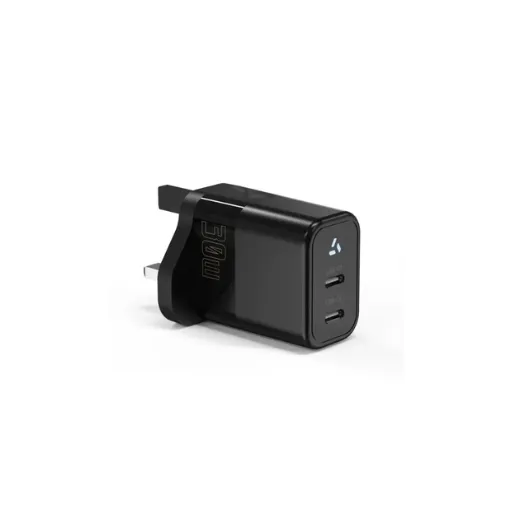 Read More
 -
What Makes a Fast Charger? A Technical Guide for OEM Buyers
June 8, 2026When the Rotterdam-based e-mobility brand VoltRide switched from 2A to 5A chargers on their 48V e-bike fleet in Q3 2024, customer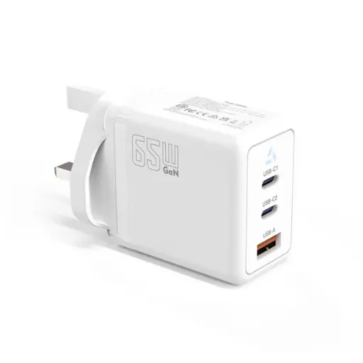 Read More
 -
USB-A vs USB-C Charging: What OEM Buyers Need to Know
June 8, 2026Your customers plug in a USB-A cable they have used for three years, and their new device takes six hours to charge. They switch t Read More
 -
QC3.0 vs QC4.0: What OEM Buyers Need to Know Before Specifying Fast Charging
June 6, 2026When Raj's team at a Bangalore-based smartphone accessories brand specified QC3.0 adapters for their 2024 power bank line, the Read More

Contact Us
Recommended Products
-
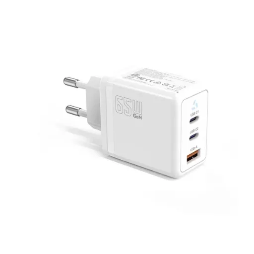
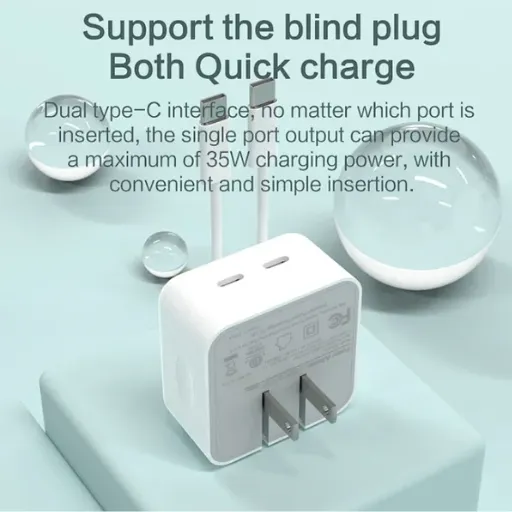
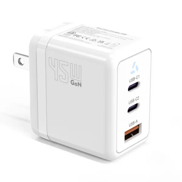
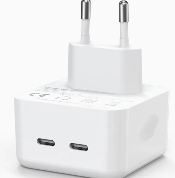
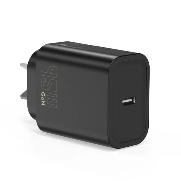
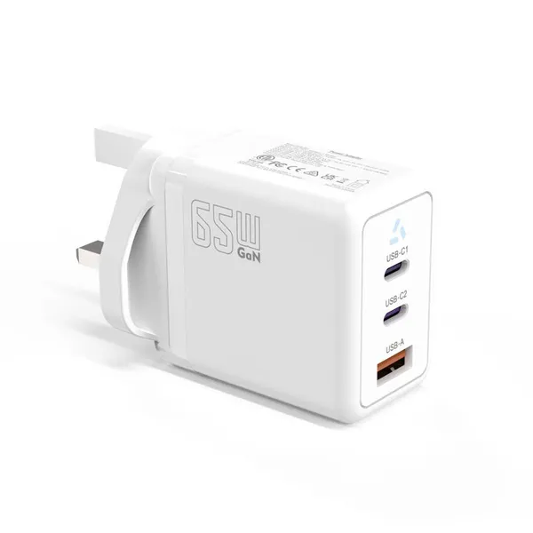
 65W USB-C GaN Wall Charger PD Fast Charging Adapter EU US Plug for Laptop Smartphone and TravelUS$ 6MOQ: 100 Pieces
 -
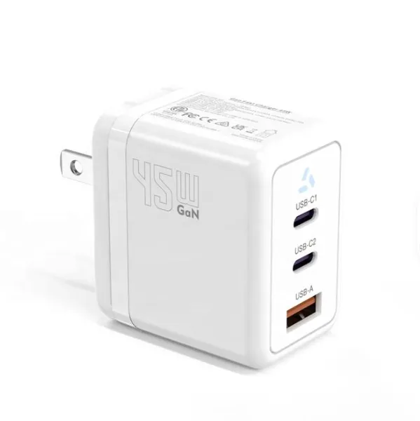
45W GaN USB-C Fast Charger JP Plug PD Wall Charging Adapter for IPhone MacBook and TabletsUS$ 8MOQ: 100 Pieces
-
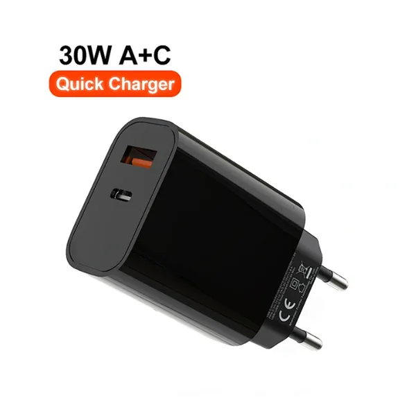
QC3.0 30W USB Fast Charger With 18W Quick Charge Wall Adapter for Android and Mobile DevicesUS$ 4MOQ: 100 Pieces
-
Compact 18W Quick Charge 3.0 USB Charger 30W Fast Charging Adapter EU US Plug for TravelUS$ 2MOQ: 100 Pieces
-
30W USB-C and USB-A PD Fast Charger Compact Wall Adapter for IPhone Samsung and IPadUS$ 3MOQ: 100 Pieces
-
35W Dual USB-C PD Charger Fast Charging Adapter for IPhone Samsung IPad and USB-C DevicesUS$ 3MOQ: 100 Pieces
-
65W USB-C GaN Charger EU Plug Fast Charging Adapter 65W USB-C PD Fast Charge Wall Charger Power Adapter for Macbook ProUS$ 5MOQ: 100 Pieces
-
65W GaN USB-C Fast Charger PD Wall Charging Adapter for Laptop IPhone and Mobile DevicesUS$ 5MOQ: 100 Pieces
-
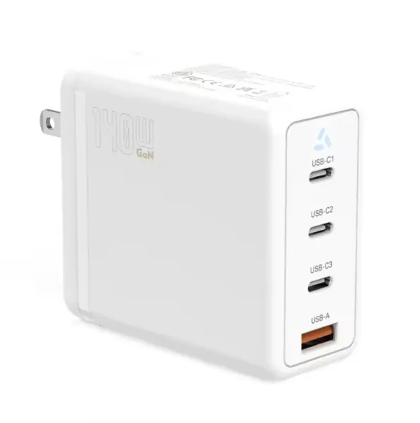
100W GaN USB-C Fast Charger With PD 3.0 for Laptop, MacBook, IPhone & Multi-Device ChargingUS$ 12MOQ: 100 Pieces
-
45W GaN USB-C Fast Charger EU AU PD Fast Wall Charging Adapter for IPhone Tablets With CE REACH PassedUS$ 8MOQ: 100 Pieces
-
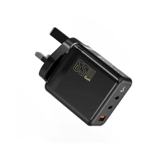
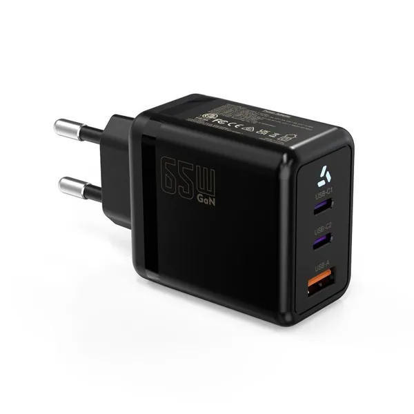
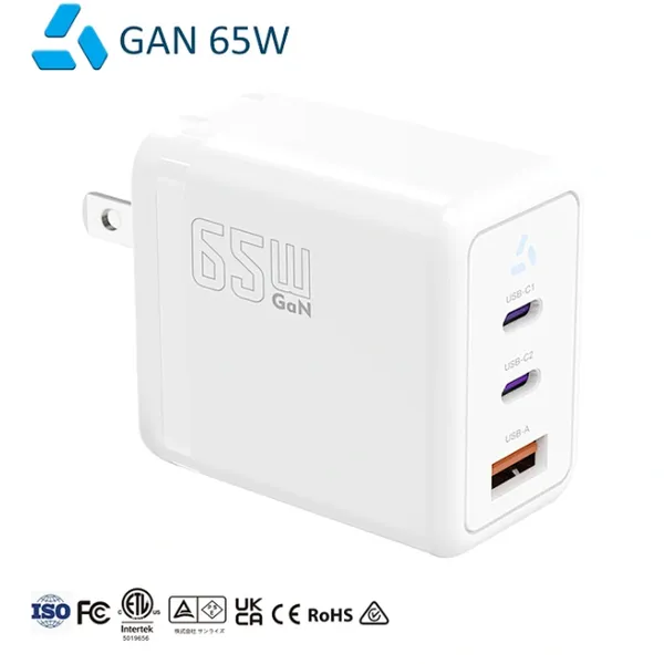
QC3.0 65W GaN USB C Super Fast Charger With UKCA 3 Ports PD 3.0 GaN Charger for Iphone Macbook SamsungUS$ 10MOQ: 100 Pieces
-
30W USB-C and USB-A GaN QC3.0 Fast Charging Adapter PD Fast Charger Compact Wall Adapter for IPhone Samsung and IPadUS$ 3MOQ: 100 Pieces
-
45W GaN USB-C Fast Charger With Dual Type-C and USB-A Ports PD Wall Charging AdapterUS$ 8MOQ: 100 Pieces
-
Dual USB C Ports QC3.0 30W Fast Charger With EU UK AU US USB-C PD Wall Chargeer 30W PD Power AdapterUS$ 3MOQ: 100 Pieces
-
Compact 65W GaN USB-C Wall Charger With Dual USB-C Ports and USB-A Fast Charging Adapter With CE UKCA ETL SAAUS$ 10MOQ: 100 Pieces
-
QC3.0 Fast Charging Adapter PD30W USB-C USB-A GaN PD Fast Charger PD 3.0 GaN Charger Compact Wall Adapter for IPhone Samsung and IPadUS$ 3MOQ: 100 Pieces
-
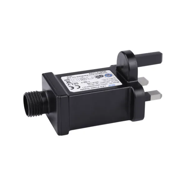
12V 5A 60W US EU AC DC Adapter LED Driver LED SMPS AC to DC Switching Power SupplyUS$ 5 - 7MOQ: 50 Pieces
-
CE FCC CUL SAA KC PSE 24Vdc 48W Switching Power Supply AdaptersUS$ 5 - 7MOQ: 50 Pieces
-
CE GS UKCA SAA CUL Qualified Waterproof Switching Power Supply Ip68 PSE UL SAA GS 12V 2AUS$ 3 - 6MOQ: 50 Pieces
-
12V 1A Factory OEM Waterproof AC Adapter for Laser Light Table Lamp ac dc Adaptor With TUV CE GS for EU MarketUS$ 5 - 7MOQ: 50 Pieces