How Does a GaN Charger Work? A Step-by-Step Circuit Guide
Your wall outlet delivers 120V or 230V AC at 50 or 60 Hz. Your laptop battery needs 20V DC. The gap between those two numbers, voltage, frequency, waveform, everything, is bridged by a switching power supply that performs one of the most elegant transformations in electronics. Do it with silicon, and the adapter is the size of a deck of cards. Do it with gallium nitride, and the same power fits in a matchbox.
This article walks through exactly how a GaN charger works, stage by stage, from the AC plug to the DC output. It explains what happens inside each circuit block of a gallium nitride charger, why GaN transistors enable each block to perform better, and what the design trade-offs mean for OEM buyers specifying adapters for production.
How Does a GaN Charger Work? The 5-Stage Answer
A GaN charger converts AC wall power to regulated DC output through five sequential stages: rectification, power factor correction, high-frequency DC-DC conversion, synchronous rectification, and feedback regulation. Gallium nitride transistors enable each stage to run at 3–10x higher switching frequency than silicon, which shrinks transformers, reduces heat, and cuts adapter volume by 30–50%.
The Big Picture: From AC Wall Power to DC Output
Every AC/DC adapter, GaN or silicon, performs the same fundamental sequence:
Rectify the AC input into rough DC
Power Factor Correct (PFC) the input current to match the voltage waveform
Switch the DC at high frequency through a transformer
Rectify and filter the transformer output into smooth DC
Regulate the output voltage against load and line variations
The difference between a GaN charger and a silicon adapter is not the sequence. It is the speed, efficiency, and size at which each step happens. GaN transistors switch 3–10x faster than silicon MOSFETs. Higher frequency means smaller magnetics, lower losses, and less heat.
Stage 1: AC Input Rectification in a GaN Charger
The AC from your wall is a sine wave swinging between positive and negative at 50 or 60 Hz. The first circuit block, the input rectifier, converts this into a unipolar (always positive) but pulsating DC voltage.
A full-bridge rectifier using four diodes flips the negative half-cycles positive. The result is a DC waveform that still ripples at 100 or 120 Hz (twice the line frequency). A bulk capacitor (typically 100–400 µF at 400V) smooths this ripple into a relatively steady DC bus voltage that feeds the rest of the GaN charger circuit.
For a 230V AC input, the rectified DC bus sits at roughly 325V. For a 120V input, it sits at roughly 170V. This high-voltage DC bus is what the switching stage sees.
How GaN Affects This Stage
GaN does not directly replace the rectifier diodes in most designs (though GaN-based synchronous rectification is emerging at the output side). What GaN enables here is a smaller input filter. Because the switching stage operates at 200–500 kHz instead of 50–100 kHz, the conducted EMI signature is higher in frequency but easier to filter with smaller common-mode chokes and X-capacitors. The input filter block shrinks by 20–30% in a well-designed GaN adapter.
Stage 2: Power Factor Correction (PFC)
In a simple rectifier, the diodes conduct only when the AC sine wave is near its peak. This draws current in narrow pulses, creating a poor power factor and harmonic distortion on the line. For adapters above 75W, regulatory standards (IEC 61000-3-2 in Europe, DOE in the U.S.) require power factor correction.
A PFC stage uses a boost converter to shape the input current into a sinusoid that tracks the input voltage. A switching transistor, traditionally a silicon MOSFET or IGBT, chops the rectified DC at high frequency through an inductor. A controller modulates the duty cycle to force the input current to follow the AC voltage waveform.
GaN in the PFC Stage
The PFC boost switch is where GaN delivers its first major advantage. A GaN HEMT (high-electron-mobility transistor) in the PFC stage can switch at 200–400 kHz versus 50–100 kHz for silicon. Higher frequency means:
Smaller boost inductor: The inductor stores energy each cycle. At 4x the frequency, it stores 1/4 the energy per cycle, so the inductor can be 1/4 the size for the same inductance value.
Lower switching losses: GaN has near-zero reverse recovery charge and low output capacitance, so the energy lost each switching transition is dramatically lower.
Higher efficiency: A GaN PFC stage typically achieves 98–99% efficiency versus 95–97% for silicon.
For a 100W adapter, that 2–3% PFC efficiency gain is 2–3W less heat before the main conversion stage even begins. Over the full adapter, the cumulative effect is a 3–5% total efficiency improvement.
Want to see how efficiency ratings affect your product certification? See our DOE Level VI compliance guide for what U.S. customs requires.
Stage 3: High-Frequency DC-DC Conversion in a GaN Charger
The PFC output is a steady high-voltage DC, roughly 390V for universal-input designs. The DC-DC stage converts this down to the target output voltage (5V, 12V, 20V, etc.) using a high-frequency transformer.
This is where the "switching" in switching power supply happens. A transistor rapidly switches the DC bus on and off, creating a square wave that drives the primary winding of a transformer. The transformer steps the voltage down (or up, in some topologies) while providing galvanic isolation between the AC line and the DC output.
Common Topologies in GaN Adapters
| Topology | Power Range | Typical Use | Why GaN Helps |
|---|---|---|---|
| Flyback | 5–100W | Low-cost adapters, chargers | Higher frequency shrinks transformer and snubber |
| LLC resonant | 60–500W | Laptop adapters, multi-port chargers | Soft switching at >200 kHz eliminates turn-on loss |
| Active clamp flyback | 30–150W | Premium single-port adapters | Recycles leakage energy, enables zero-voltage switching |
| Dual-active bridge | 100W–kW | High-power, bidirectional | GaN enables compact designs at very high power |
Flyback: The Workhorse Topology
In a flyback converter, the transformer also acts as an inductor. When the switch turns on, current ramps up in the primary winding, storing energy in the transformer core. When the switch turns off, the magnetic field collapses, and the secondary winding delivers that energy to the output through a diode.
In a silicon flyback, the switching transistor operates at 50–100 kHz. The transformer core must be large enough to store the energy without saturating at that frequency. The output diode must handle the reverse recovery stress each cycle.
In a GaN flyback, the transistor switches at 200–400 kHz. The transformer stores less energy per cycle, so the core can be smaller. A smaller core means fewer copper windings, less copper loss, and a transformer that is 30–40% smaller by volume. The output rectifier is typically replaced by a synchronous rectifier MOSFET for even higher efficiency.
LLC Resonant: The Premium Topology
Higher-power GaN adapters (65W and above) often use an LLC resonant half-bridge topology. In an LLC converter, the transformer primary is part of a resonant tank circuit (inductor + capacitor). The switches operate at a frequency near the tank's resonant frequency, enabling zero-voltage switching (ZVS).
ZVS means the transistor turns on exactly when the voltage across it is zero. This eliminates turn-on switching loss, one of the largest loss mechanisms in hard-switched converters. GaN HEMTs are ideal for LLC because:
Their low output capacitance (Coss) makes ZVS easier to achieve across a wide load range
Their high switching speed allows the resonant tank to operate above 200 kHz
Their low gate charge reduces gate drive losses
An LLC GaN adapter at 100W can achieve peak efficiencies of 93–94%, compared to 89–91% for a silicon LLC design. The transformer in a 100W GaN LLC design is roughly half the volume of its silicon equivalent.
Stage 4: Synchronous Rectification and Output Filtering
The transformer secondary delivers a high-frequency AC waveform (square wave or resonant sine wave, depending on topology). This must be rectified back to DC and filtered before reaching the output.
In older designs, a Schottky diode handles this rectification. Schottky diodes are fast and have low forward voltage, but they still drop 0.3–0.5V. At 20A output, that is 6–10W of pure loss.
Modern GaN adapters, and many high-efficiency silicon adapters, use synchronous rectification. A MOSFET (silicon or GaN) replaces the diode. The MOSFET is turned on during the conduction interval and off during the blocking interval, controlled by a synchronous rectifier controller that senses the transformer voltage. A MOSFET with 5 mΩ on-resistance at 20A drops only 0.1V, saving 4–8W compared to a diode.
Output Filtering
After rectification, the DC still contains ripple at the switching frequency. An LC filter (inductor + capacitor) smooths this into a clean DC output with ripple typically below 100 mV. Because GaN adapters switch at higher frequencies, the filter components are smaller:
Higher switching frequency means lower ripple amplitude for the same filter
Or equivalently, smaller inductance and capacitance for the same ripple target
A GaN adapter's output filter is typically 20–30% smaller than a silicon adapter's filter at the same power level.
Stage 5: Feedback and Regulation
The output voltage must stay constant regardless of input voltage changes (90–264V universal input) and load changes (0–100%). A feedback loop senses the output voltage, compares it to a reference, and adjusts the switching duty cycle or frequency to maintain regulation.
An optocoupler provides isolated feedback across the galvanic barrier. The secondary-side controller senses the output voltage and drives the optocoupler LED. The primary-side controller reads the optocoupler signal and adjusts the gate drive to the switching transistor.
GaN-Specific Controller Considerations
GaN HEMTs have different gate characteristics than silicon MOSFETs. Their threshold voltage is lower (typically 1.5–2.5V versus 3–4V for silicon). Their gate can be damaged by voltages above 6V. They switch so fast that PCB layout parasitics, trace inductance of just a few nanohenries, can cause destructive voltage overshoot.
This means GaN adapters require controllers and gate drivers designed specifically for GaN. Key requirements:
Tight gate voltage regulation: The driver must hold gate voltage within a narrow window (typically 5V ± 0.5V)
Fast, clean drive strength: Rise and fall times under 5 ns to minimize switching loss
Integrated protection: UVLO (under-voltage lockout), over-current protection, and shoot-through prevention
Optimized PCB layout: Minimized loop inductance in the gate drive and power stage
When evaluating a GaN adapter supplier, ask whether they use a GaN-optimized controller IC or a generic controller with external level shifters. Integrated GaN power ICs, where the GaN transistor and driver are co-packaged, offer the best reliability and smallest footprint. Texas Instruments publishes detailed application notes on GaN gate drive best practices that any design team should review. Anenerge's GaN platforms use integrated GaN power ICs from established semiconductor vendors, eliminating the layout risks of discrete GaN designs.
Need a GaN adapter designed for your specific output and connector? Our OEM/ODM services support custom GaN designs from 30W to 150W with private-label enclosures and branding.
What Happens Inside the GaN Transistor Itself

The circuit stages above describe the system. But what actually happens inside the GaN transistor during each switching cycle?
The Physics in Plain Terms
A GaN HEMT is built on a silicon substrate with a thin layer of gallium nitride deposited on top. At the interface between GaN and an aluminum gallium nitride (AlGaN) barrier layer, a two-dimensional electron gas (2DEG) forms. This is a sheet of highly mobile electrons trapped at the interface.
The 2DEG gives GaN two critical advantages:
Electron mobility: Electrons in the 2DEG move roughly 1,000x faster than in silicon. Higher mobility means lower resistance when the transistor is on (low Rds(on)).
Switching speed: Because the channel is extremely thin and the electrons are already present (no need to inject carriers), the transistor turns on and off in nanoseconds instead of tens of nanoseconds.
Low On-Resistance
On-resistance (Rds(on)) is the resistance between drain and source when the transistor is fully on. Lower Rds(on) means less conduction loss (loss = I² × R). GaN achieves lower Rds(on) per unit area than silicon, meaning a smaller die can handle the same current with less loss.
For a 65W adapter's primary switch, a GaN HEMT might have 150 mΩ Rds(on) in a 3 mm × 3 mm package. A silicon MOSFET with comparable voltage rating (650V) would need a larger die to achieve the same Rds(on), or would run at higher resistance and generate more heat.
Zero Reverse Recovery
Silicon MOSFETs contain a body diode that conducts when the transistor is off and the voltage reverses. When the transistor turns on again, the body diode must recover, a process that creates a reverse recovery current spike and associated loss. This is a major limitation in hard-switched converters.
GaN HEMTs have no body diode. They can conduct in reverse through the 2DEG channel, but there is no minority carrier injection and therefore no reverse recovery charge. This eliminates reverse recovery loss entirely, a significant advantage in hard-switched topologies like flyback and boost PFC.
Low Output Capacitance
The output capacitance (Coss) of a transistor is the capacitance between drain and source. Every switching cycle, the driver must charge and discharge this capacitance. The energy stored is ½ × Coss × V². At 400V bus voltage, this energy becomes significant.
GaN HEMTs have roughly 3–5x lower Coss than silicon MOSFETs of the same Rds(on) and voltage rating. Lower Coss means:
Less energy lost charging/discharging each cycle
Easier zero-voltage switching in resonant topologies
Higher switching frequency without excessive loss
Thermal Management in GaN Adapters
GaN transistors generate less heat than silicon, but they are also more sensitive to temperature. The 2DEG channel degrades at sustained temperatures above 150°C, and the threshold voltage drifts with temperature. Proper thermal design is critical.
Heat Path Design
In a typical GaN adapter, heat flows from the transistor die through the package, into a copper pad on the PCB, and then to the enclosure or a heatsink. Because GaN adapters often omit traditional heatsinks (relying on the PCB copper and enclosure alone), the thermal path must be carefully engineered.
Copper area: The PCB pad under the GaN device may be 50–100 mm² of copper, sometimes with thermal vias to inner layers
Enclosure conduction: The PCB is often thermally coupled to the adapter's plastic or metal enclosure
Airflow: Natural convection is usually sufficient for GaN adapters below 100W
At Anenerge, every GaN adapter design undergoes thermal simulation before prototyping. The GaN device, transformer, output rectifier, and PFC inductor are all modeled together to ensure no component exceeds its rated temperature at full load and maximum ambient.
When Chen, an engineering lead at a Shenzhen consumer electronics brand, first sampled a GaN adapter for his 65W laptop charger project, he was concerned about surface temperature. His previous silicon adapter ran at 68°C surface temperature under full load. The GaN sample measured 48°C at the same load, cool enough that his industrial design team could use a sealed enclosure without ventilation holes, improving the product's IP rating and aesthetic.
EMI Considerations with GaN
Higher switching frequency raises a concern: electromagnetic interference (EMI). A transistor switching at 400 kHz generates harmonics at 800 kHz, 1.2 MHz, 1.6 MHz, and beyond. If not controlled, these harmonics can interfere with radios, televisions, and other electronics.
Conducted EMI
Conducted EMI travels back out through the AC power cord. It is controlled by:
Common-mode choke: A toroidal inductor on the AC input that blocks high-frequency common-mode noise
X-capacitors: Capacitors across the AC line that shunt differential noise
Y-capacitors: Capacitors from line/neutral to ground that shunt common-mode noise
Shielding: A copper or aluminum shield between the transformer primary and secondary
GaN adapters can meet the same EMI standards as silicon adapters (EN 55032 Class B, FCC Part 15 Class B) but require careful design. According to Power Electronics News, the GaN power device market is projected to grow significantly as higher-frequency designs become standard across consumer and industrial applications. The faster edge rates of GaN switching generate higher-frequency harmonics, so the filter must be effective at those frequencies. The good news: smaller filters can be effective at higher frequencies, so the total EMI filter size does not necessarily increase.
Radiated EMI
Radiated EMI travels through the air. It is controlled by PCB layout (minimizing loop areas), shielding, and snubber circuits. GaN's fast switching can increase radiated EMI if the PCB layout is poor. A well-designed GaN adapter uses:
Minimized switching node copper area (reduces antenna effect)
Ground planes beneath high-frequency traces
Proper shielding of the transformer
RC snubbers where needed to damp high-frequency ringing
Need GaN adapters with full EMI pre-compliance? Anenerge designs every GaN platform to pass EN 55032 and FCC Part 15 Class B before third-party testing. Request a sample with your target power and connector spec.
GaN Charger Operation: A Complete Example
Let us trace the complete operation of a 65W GaN USB-C PD adapter delivering 20V at 3.25A to a laptop.
The Sequence
Plug-in: 230V AC (or 120V AC) enters through the AC plug and fuse. The full-bridge rectifier converts it to pulsating DC. The bulk capacitor smooths it to ~325V DC (or ~170V DC).
PFC stage: The boost converter shapes the input current into a sinusoid. The GaN boost switch chops at 200 kHz. The PFC controller adjusts duty cycle to maintain a 390V DC bus. Input current THD (total harmonic distortion) stays below 10%, meeting IEC 61000-3-2 Class D.
DC-DC stage: The LLC resonant half-bridge switches at 250–350 kHz, varying frequency to regulate output. The GaN half-bridge transistors achieve zero-voltage switching across most of the load range. The transformer steps 390V down to ~22V AC on the secondary.
Synchronous rectification: Two GaN or silicon MOSFETs on the secondary side act as rectifiers, turning on and off in sync with the transformer voltage. A synchronous rectifier controller manages the timing.
Output filter: An LC filter smooths the rectified DC to <100 mV ripple. The output is 20.0V DC.
Feedback loop: A USB-C PD controller communicates with the laptop, negotiating 20V at 3.25A. A voltage divider and error amplifier sense the output. An optocoupler sends the error signal back to the primary-side controller, which adjusts the LLC switching frequency to maintain 20V.
Protection: The adapter monitors for over-voltage, over-current, over-temperature, and short-circuit conditions. If any limit is exceeded, the controller shuts down the GaN switches within microseconds.
The entire conversion from AC wall power to regulated DC happens in a package measuring roughly 50 mm × 50 mm × 30 mm, something silicon could not achieve at this power level without a fan or a large heatsink.
How GaN Enables Higher Power Density
Power density is the ratio of output power to adapter volume, measured in watts per cubic centimeter (W/cm³). A typical silicon adapter achieves 0.3–0.5 W/cm³. A GaN adapter achieves 0.8–1.2 W/cm³ or higher.
The improvement comes from multiple factors working together:
| Factor | Silicon Adapter | GaN Adapter | Impact on Size |
|---|---|---|---|
| Switching frequency | 50–100 kHz | 200–500 kHz | Smaller transformer and filters |
| Switching losses | Higher per cycle | Lower per cycle | Less heatsinking needed |
| Transformer core size | Larger | 30–40% smaller | Direct volume reduction |
| Filter components | Larger | 20–30% smaller | Direct volume reduction |
| EMI filter | Larger | Comparable or smaller | No size penalty |
The cumulative effect is a GaN charger that delivers the same power in roughly half the volume of a silicon equivalent. For OEM buyers, this translates into smaller retail packaging, lower freight costs, and a product that consumers perceive as more premium.
GaN vs Silicon: Inside the Switching Waveform
The difference between GaN and silicon is visible on an oscilloscope. When a silicon MOSFET turns on, the voltage falls and current rises over 20–50 ns. During this transition, both voltage and current are high simultaneously, creating a power loss spike.
When a GaN HEMT turns on, the transition completes in 2–5 ns. The overlap between voltage and current is dramatically shorter, so the switching loss, the integral of V × I during the transition, is 3–5x smaller.
This faster switching also reduces the size of the "snubber" circuits that protect the transistor from voltage overshoot. In a silicon flyback, the snubber may dissipate 1–2W. In a GaN flyback, the snubber can be smaller or eliminated, recovering that loss.
Key Takeaways: How GaN Changes Adapter Design

Higher frequency enables smaller magnetics: A GaN transformer at 300 kHz is roughly one-third the size of a silicon transformer at 60 kHz for the same power
Lower switching losses improve efficiency: GaN switching loss is 3–5x lower than silicon, adding 3–5 percentage points to total adapter efficiency
Zero reverse recovery eliminates body diode loss: GaN HEMTs have no body diode, removing a major loss mechanism in hard-switched converters
Integrated GaN ICs simplify design: Co-packaged GaN transistors and drivers reduce PCB layout risk and component count
Thermal design still matters: GaN reduces heat but does not eliminate it; proper thermal simulation and copper area are essential
EMI requires attention: Faster switching creates higher-frequency harmonics, but careful layout and filtering maintain compliance
When Priya, a procurement engineer at a U.S. IoT brand, reviewed the teardown of a GaN adapter versus her current silicon design, the difference was unmistakable. The GaN board had half the component count. The transformer was a quarter of the volume. The heatsink was gone entirely. Her product team had been struggling to fit a 65W adapter inside a compact router enclosure for months. The GaN design solved the thermal and space constraints in a single platform change.
Next Steps
Understanding how a GaN charger works is the first step. Evaluating one for your product is the second. The difference between GaN and silicon is not just on paper, it is immediately apparent in size, weight, and surface temperature when you hold the two side by side.
If you are specifying GaN chargers or AC/DC adapters for a product launch and want to understand whether GaN fits your power, size, and cost targets, the most direct path is to evaluate a sample.
Send us your output voltage, current, connector type, and target certifications. Our engineering team will recommend the right GaN platform, flyback or LLC, single-port or multi-port, and ship a sample for evaluation within one week. For custom designs, we return a full proposal with circuit topology, efficiency projection, thermal simulation, and BOM estimate within 48 hours.
Request a free GaN adapter sample or get an OEM quote for your next product generation.
Recently Posted
-
Why Is My Fast Charger Not Charging Fast? 7 Technical Reasons Explained
June 8, 2026Last March, a product manager at a Rotterdam e-bike brand called us with a problem we see at least twice a quarter. Their new 48V Read More
 -
What Makes a Fast Charger? A Technical Guide for OEM Buyers
June 8, 2026When the Rotterdam-based e-mobility brand VoltRide switched from 2A to 5A chargers on their 48V e-bike fleet in Q3 2024, customer Read More
 -
USB-A vs USB-C Charging: What OEM Buyers Need to Know
June 8, 2026Your customers plug in a USB-A cable they have used for three years, and their new device takes six hours to charge. They switch t Read More
 -
QC3.0 vs QC4.0: What OEM Buyers Need to Know Before Specifying Fast Charging
June 6, 2026When Raj's team at a Bangalore-based smartphone accessories brand specified QC3.0 adapters for their 2024 power bank line, the Read More

Contact Us
Recommended Products
-
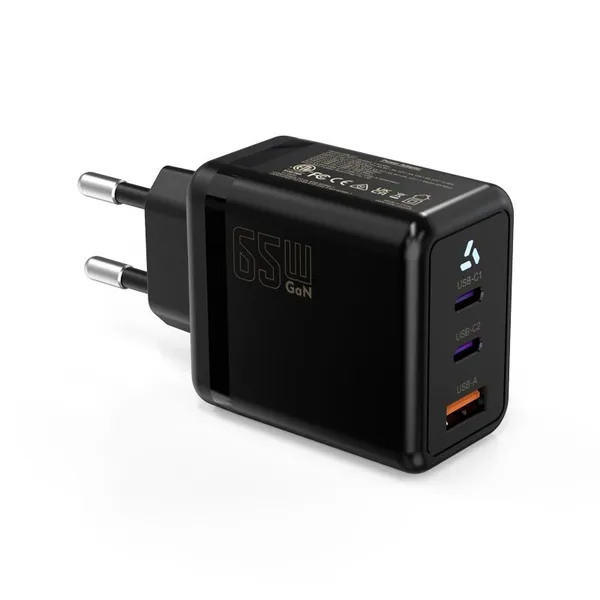
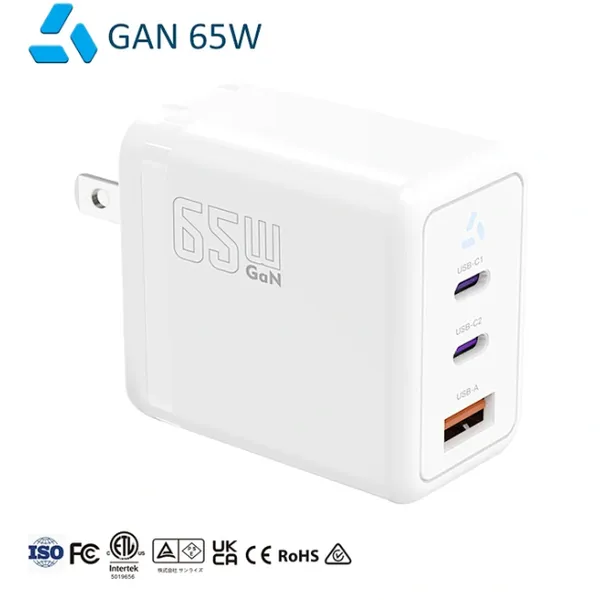
 65W USB-C GaN Wall Charger PD Fast Charging Adapter EU US Plug for Laptop Smartphone and TravelUS$ 6MOQ: 100 Pieces
 -
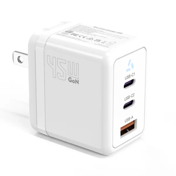
45W GaN USB-C Fast Charger JP Plug PD Wall Charging Adapter for IPhone MacBook and TabletsUS$ 8MOQ: 100 Pieces
-
QC3.0 30W USB Fast Charger With 18W Quick Charge Wall Adapter for Android and Mobile DevicesUS$ 4MOQ: 100 Pieces
-
Compact 18W Quick Charge 3.0 USB Charger 30W Fast Charging Adapter EU US Plug for TravelUS$ 2MOQ: 100 Pieces
-
30W USB-C and USB-A PD Fast Charger Compact Wall Adapter for IPhone Samsung and IPadUS$ 3MOQ: 100 Pieces
-
35W Dual USB-C PD Charger Fast Charging Adapter for IPhone Samsung IPad and USB-C DevicesUS$ 3MOQ: 100 Pieces
-
65W USB-C GaN Charger EU Plug Fast Charging Adapter 65W USB-C PD Fast Charge Wall Charger Power Adapter for Macbook ProUS$ 5MOQ: 100 Pieces
-
65W GaN USB-C Fast Charger PD Wall Charging Adapter for Laptop IPhone and Mobile DevicesUS$ 5MOQ: 100 Pieces
-
100W GaN USB-C Fast Charger With PD 3.0 for Laptop, MacBook, IPhone & Multi-Device ChargingUS$ 12MOQ: 100 Pieces
-
45W GaN USB-C Fast Charger EU AU PD Fast Wall Charging Adapter for IPhone Tablets With CE REACH PassedUS$ 8MOQ: 100 Pieces

-
QC3.0 65W GaN USB C Super Fast Charger With UKCA 3 Ports PD 3.0 GaN Charger for Iphone Macbook SamsungUS$ 10MOQ: 100 Pieces
-
30W USB-C and USB-A GaN QC3.0 Fast Charging Adapter PD Fast Charger Compact Wall Adapter for IPhone Samsung and IPadUS$ 3MOQ: 100 Pieces
-
45W GaN USB-C Fast Charger With Dual Type-C and USB-A Ports PD Wall Charging AdapterUS$ 8MOQ: 100 Pieces
-
Dual USB C Ports QC3.0 30W Fast Charger With EU UK AU US USB-C PD Wall Chargeer 30W PD Power AdapterUS$ 3MOQ: 100 Pieces
-
Compact 65W GaN USB-C Wall Charger With Dual USB-C Ports and USB-A Fast Charging Adapter With CE UKCA ETL SAAUS$ 10MOQ: 100 Pieces


-
QC3.0 Fast Charging Adapter PD30W USB-C USB-A GaN PD Fast Charger PD 3.0 GaN Charger Compact Wall Adapter for IPhone Samsung and IPadUS$ 3MOQ: 100 Pieces
-
12V 5A 60W US EU AC DC Adapter LED Driver LED SMPS AC to DC Switching Power SupplyUS$ 5 - 7MOQ: 50 Pieces
-
CE FCC CUL SAA KC PSE 24Vdc 48W Switching Power Supply AdaptersUS$ 5 - 7MOQ: 50 Pieces
-
CE GS UKCA SAA CUL Qualified Waterproof Switching Power Supply Ip68 PSE UL SAA GS 12V 2AUS$ 3 - 6MOQ: 50 Pieces
-
12V 1A Factory OEM Waterproof AC Adapter for Laser Light Table Lamp ac dc Adaptor With TUV CE GS for EU MarketUS$ 5 - 7MOQ: 50 Pieces