What Is a GaN Charger? A Technical Guide for OEM Buyers
A 65W power supply that fits in the palm of your hand used to be impossible. Conventional silicon adapters at that power rating were bulky, heavy, and ran hot enough to warm a desk. Then gallium nitride changed the rules.
GaN chargers are now the default for premium laptop adapters, fast-charging phone bricks, and compact travel power supplies. For OEM brand owners and procurement engineers, the shift from silicon to GaN is not just a consumer trend — it is a design decision that affects thermal budgets, enclosure sizes, shipping weights, and energy efficiency ratings.
This article explains what a GaN charger actually is, how gallium nitride semiconductors differ from traditional silicon MOSFETs, and what specifications OEM buyers should verify before placing a production order. It draws on Anenerge's experience designing GaN-based adapters for consumer electronics, IoT, and portable power applications.
What "GaN" Actually Means
GaN stands for gallium nitride, a wide-bandgap semiconductor material that replaces silicon in the switching transistors of a power adapter. In a standard AC/DC adapter, power passes through a rectifier, a switching stage, a transformer, and an output filter. The switching stage is where the conversion happens, and it is also where most of the losses occur.
Silicon MOSFETs have been the industry standard for decades. They are reliable, cheap, and well understood. But silicon has physical limits: electron mobility is finite, switching frequencies are capped by switching losses, and heat generation scales with frequency. Gallium nitride has roughly 1,000 times the electron mobility of silicon and can switch at frequencies 3–10x higher with lower switching losses.
Why Higher Switching Frequency Matters
Higher switching frequency means the transformer and filter components can be smaller. A transformer operating at 100 kHz needs less core material and fewer copper windings than one operating at 50 kHz. The same applies to output capacitors and inductors. The result: a GaN adapter can deliver the same output power in a package 30–50% smaller than a silicon equivalent.
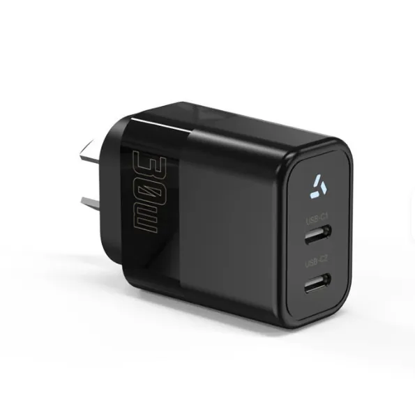
At Anenerge, our 65W GaN USB-C adapter platform measures roughly 50 mm x 50 mm x 30 mm. A comparable silicon adapter at the same power rating is typically 70 mm x 70 mm x 35 mm or larger. For OEM buyers shipping adapters in retail boxes, that size difference translates directly into lower freight costs and more compact packaging.
GaN Charger vs Silicon Adapter: The Key Differences
The table below summarizes the practical differences between GaN and silicon adapters at the same power rating:
| Parameter | Silicon Adapter | GaN Adapter |
|---|---|---|
| Typical size (65W) | 70 x 70 x 35 mm | 50 x 50 x 30 mm |
| Typical weight | 180–220 g | 90–120 g |
| Switching frequency | 50–100 kHz | 200–500 kHz |
| Peak efficiency | 87–90% | 91–94% |
| Operating temperature | 50–70°C surface | 40–55°C surface |
| No-load power draw | 0.15–0.30W | 0.10–0.20W |
| Cost at volume | Lower baseline | 10–20% premium |
Efficiency and Thermal Performance
GaN transistors switch faster with lower gate charge, which reduces switching losses during each cycle. Lower losses mean less heat. Less heat means smaller heatsinks, or in many cases, no heatsink at all. The adapter runs cooler, lasts longer, and wastes less energy.
For a brand owner shipping 50,000 laptop adapters per year, a 3% efficiency gain from 90% to 93% translates into measurable energy savings. At 65W output, 3% higher efficiency saves roughly 2W per unit. Across 50,000 units running 8 hours per day, that is 292 MWh saved annually. At $0.12/kWh, that is $35,000 in energy cost reduction — and a stronger story for the brand's sustainability report.
Size and Portability
When Marcus, a product manager at a European portable electronics brand, switched his product line from silicon 45W adapters to GaN equivalents in early 2025, the difference was stark. The retail box shrank by 40%. Shipping cartons went from 24 units per box to 36 units per box.
Freight cost per unit dropped by 18%. End customers noticed, too. Reviews mentioned the "surprisingly compact charger" as a selling point. The GaN premium at the BOM level paid back in under six months through logistics savings alone.
How GaN Technology Works Inside the Adapter
Understanding the physics is not required to buy a GaN charger, but understanding the design implications is. Here is what happens inside the adapter.
Wide Bandgap Explained
Semiconductors have a property called the bandgap — the energy difference between a material's valence band and conduction band. Silicon has a bandgap of approximately 1.1 eV. Gallium nitride has a bandgap of approximately 3.4 eV. This wider gap means GaN can handle higher voltages, operate at higher temperatures, and switch faster before breakdown occurs.
Lower On-Resistance and Gate Charge
GaN HEMTs (high-electron-mobility transistors) have lower on-resistance (Rds(on)) per unit area than silicon MOSFETs. Lower on-resistance means lower conduction losses when the transistor is conducting current. Lower gate charge means less energy is needed to switch the transistor on and off. Both properties contribute to higher efficiency, especially at high switching frequencies.
The Role of the Controller and Driver
GaN transistors require specialized gate drivers. The driver must supply fast, clean pulses with tight voltage tolerances. A poorly matched driver can cause ringing, overshoot, or shoot-through, damaging the transistor or generating excessive EMI. Quality GaN adapters use controllers designed specifically for GaN switching, not repurposed silicon controllers.
When evaluating a GaN adapter supplier, ask whether the design uses a GaN-optimized controller or a generic controller with external drivers. The former typically delivers better efficiency and reliability. Anenerge's GaN platforms use dedicated GaN power ICs with integrated drivers, minimizing component count and improving consistency at volume.
What to Look for in a GaN Charger for OEM Production
Not all GaN adapters are created equal. The presence of a GaN transistor does not guarantee good performance. Here are the specifications OEM buyers should verify.
1. Output Power and Voltage Range
GaN technology shines at medium-to-high power densities. Typical applications include:
30W–65W: Phone, tablet, and lightweight laptop adapters
65W–100W: Laptop and high-power device adapters
100W–240W: Gaming laptops, workstations, and multi-port chargers
Verify the output voltage and current match your device's input requirements. USB-C Power Delivery (PD) adapters typically support 5V, 9V, 12V, 15V, and 20V profiles with variable current. Fixed-output adapters (e.g. 12V 5A) are also available in GaN designs for non-PD applications.
2. Efficiency Certification
GaN adapters should still meet the same regulatory standards as silicon adapters. Verify:
DOE Level VI for the U.S. market (mandatory since 2016)
ErP Tier V for the EU market
ENERGY STAR Level V for sustainability-focused brands
The higher baseline efficiency of GaN makes these certifications easier to achieve, but do not assume compliance. Request current test reports with traceable report numbers. For more detail, see our DOE Level VI compliance guide.
3. Thermal Design and Operating Temperature
GaN adapters run cooler, but they still generate heat. Verify the adapter's rated operating temperature range and the ambient temperature used for testing. A well-designed GaN adapter should operate reliably from 0°C to +40°C ambient, with derating up to +50°C or +60°C for industrial applications.
Ask the supplier for thermal imaging data or surface temperature measurements at full load. Surface temperatures above 60°C at 25°C ambient suggest marginal thermal design, even with GaN.
4. EMI and Safety Certifications
Higher switching frequencies can generate more electromagnetic interference (EMI) if the filter design is inadequate. Verify the adapter has passed:
Conducted EMI: EN 55032 / CISPR 32 Class B
Radiated EMI: EN 55032 / CISPR 32 Class B
Safety: UL 62368-1, IEC 62368-1, or EN 62368-1
The GaN transistor itself does not create EMI. Poor PCB layout, inadequate shielding, or a skimped filter stage does. Reputable manufacturers address EMI during the design phase, not as an afterthought.
5. Component Quality and Supplier Traceability
GaN semiconductors are sourced from a smaller pool of suppliers than silicon MOSFETs. Major GaN device manufacturers include Infineon, Navitas, GaN Systems, Transphorm, and Power Integrations. Ask your adapter supplier which GaN devices they use and whether they have second-source options.
Lead times for GaN devices can fluctuate more than silicon. A supplier with multiple qualified GaN sources is better positioned to maintain production continuity.
Common Myths About GaN Chargers
Myth 1: GaN Is Only for High-Power Adapters
GaN is most visible in 65W+ laptop chargers, but the technology scales down effectively. 20W and 30W GaN phone chargers are now common, offering the same size and efficiency benefits at lower power. For OEMs building compact IoT or portable device adapters, GaN is viable even below 30W.
Myth 2: GaN Adapters Are Unreliable
Early GaN adapters had teething problems, primarily related to gate driver design and PCB layout. Those issues have been largely resolved by dedicated GaN power ICs and mature reference designs from major semiconductor vendors. Modern GaN adapters have field reliability comparable to silicon, with the added benefit of lower thermal stress.
Myth 3: GaN Replaces the Need for Good Thermal Design
GaN reduces losses, but it does not eliminate them. A poorly designed GaN adapter can still overheat if the thermal path is inadequate, the transformer is undersized, or the enclosure blocks airflow. GaN is an enabler of smaller adapters, not an excuse to skip thermal validation.
When Anenerge's engineering team designs a GaN adapter, we run finite-element thermal simulation before the first prototype is built. The GaN transistor is only one part of a system that includes the transformer, output rectifier, filter capacitors, and enclosure. Every component must be sized for the application's duty cycle and ambient conditions.
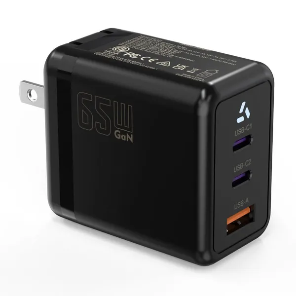
GaN in Multi-Port and High-Power Adapters
One of the most compelling applications for GaN is multi-port adapters. A 100W GaN charger with two USB-C ports and one USB-A port can intelligently distribute power across devices. When only one device is connected, it receives the full 100W. When multiple devices connect, the adapter splits power according to negotiated PD profiles.
This dynamic power allocation requires precise current sensing and fast switching — both areas where GaN excels. Silicon adapters at the same power level struggle to match the size and thermal performance of multi-port GaN designs.
For OEM buyers considering multi-port adapter SKUs, GaN is increasingly the only practical path above 65W total output. The alternative is a larger, heavier silicon design that consumers and reviewers reject.
Cost Considerations for OEM Buyers
GaN adapters carry a BOM premium over silicon. The exact delta depends on power level, volume, and design complexity. As of mid-2026, expect roughly:
10–15% premium at 30–65W
15–20% premium at 65–100W
20–25% premium at 100W+ or multi-port designs
When the Premium Pays Back
The GaN premium is easiest to justify when:
Freight and packaging matter: Smaller adapters reduce DIM weight and allow more units per carton
Thermal budgets are tight: Compact enclosures or sealed designs with limited airflow
Efficiency ratings are marketing requirements: ENERGY STAR, EPEAT, or corporate sustainability targets
Retail shelf presence matters: Consumers notice and compare adapter size
Multi-port configurations are needed: GaN enables power distribution silicon cannot match at the same size
When Silicon Still Makes Sense
Silicon remains the right choice when:
Cost is the primary driver: Budget consumer products where every cent counts
Power levels are low: Below 20W, the size and efficiency benefits of GaN are marginal
Designs are mature and shipping: Legacy products with no plans for redesign
Thermal headroom is abundant: Open-frame or fan-cooled designs where size is not constrained
GaN and the Future of Power Adapter Design
The shift from silicon to GaN in power adapters is following a predictable adoption curve. Consumer electronics led the way. Enterprise laptops and tablets followed. Industrial and IoT applications are now catching up.
Higher Power Density Trends
Next-generation GaN devices are pushing switching frequencies above 1 MHz in some designs. This enables even smaller transformers and filters, though EMI filtering becomes more challenging. Expect 100W adapters in packages smaller than today's 65W designs within the next product generation.
Integration with USB-C PD 3.1
USB-C Power Delivery 3.1 extends the standard to 240W at 48V, enabling GaN adapters to power high-performance laptops, gaming systems, and even small appliances. For OEM buyers, this means a single adapter platform can serve multiple product categories, reducing SKU complexity.
Regulatory Pressure on Efficiency
DOE Level VI and ErP Tier V are baseline requirements today. Future standards — including a potential DOE Level VII — will demand even lower no-load power and higher active-mode efficiency. GaN's inherent efficiency advantage positions it well for stricter regulations.
At Anenerge, our GaN adapter platform already targets 93%+ efficiency at full load and <0.15W no-load draw, giving headroom against anticipated standard revisions. See our DOE Level VI feature page for current efficiency documentation.
Anenerge GaN Adapter Capabilities
Anenerge designs and manufactures GaN-based AC/DC adapters for OEM brand owners across consumer electronics, IoT, and portable power segments. Our current GaN platform includes:
Power range: 30W to 150W in single and multi-port configurations
Output profiles: USB-C PD 3.0/3.1, fixed DC output, and custom voltage/current combinations
Form factors: Wall-mount (folding and fixed plug), desktop, and in-line
Plug options: US, EU, UK, AU, interchangeable, and custom tooled options
Efficiency: 91–94% peak, with DOE Level VI and ErP Tier V compliance
Safety: UL, TUV, CB, CE, UKCA, FCC certifications available
Want to evaluate a GaN adapter for your product line? Request a free sample with your target power, voltage, and connector spec. Engineering samples ship within 7 days for standard configurations.
Our OEM/ODM services support custom GaN designs including private-label enclosures, silk-screen branding, and retail packaging. Bring your product requirements and we will propose a GaN platform matched to your thermal, size, and cost targets.
Key Takeaways for OEM Buyers
GaN is a material change, not a marketing label: Gallium nitride transistors replace silicon MOSFETs to enable higher switching frequency, lower losses, and smaller size
Size and efficiency are the primary benefits: 30–50% smaller adapters with 3–5% higher efficiency translate into freight savings, cooler operation, and better user experience
Certification still matters: GaN does not exempt an adapter from DOE Level VI, ErP Tier V, or safety standards. Verify test reports
Not every application needs GaN: Below 20W or in cost-driven, thermally unconstrained designs, silicon may still be the right choice
Supplier GaN expertise varies: Ask about controller choice, GaN device sourcing, thermal validation, and EMI test results
When Elena, a procurement manager at a U.S. IoT brand, first evaluated GaN for her company's next-gen router adapter, she was skeptical. The 15% BOM premium seemed hard to defend.
Then she ran the numbers. The smaller adapter eliminated the need for a separate power brick compartment in the retail box. It cut freight costs by 22% and helped the product earn ENERGY STAR qualification. The GaN adapter became the default for the entire product line. That was March 2025. She has not shipped a silicon adapter since.
Next Steps
If you are sourcing AC/DC adapters for a product launch and considering GaN, the next step is to compare real samples. Request a GaN adapter and a silicon equivalent at your target power level. Test them side by side for size, weight, surface temperature, and no-load power draw.
The difference is immediately obvious.
Send us your output voltage, current, connector type, and target certifications. Our engineering team will recommend the right GaN or silicon platform and ship a sample for evaluation within one week. For custom designs, we return a proposal with charge curve, efficiency data, and thermal profile within 48 hours.
Request a free GaN adapter sample or get an OEM quote for your next product generation.
Recently Posted
-
Why Is My Fast Charger Not Charging Fast? 7 Technical Reasons Explained
June 8, 2026Last March, a product manager at a Rotterdam e-bike brand called us with a problem we see at least twice a quarter. Their new 48V Read More
 -
What Makes a Fast Charger? A Technical Guide for OEM Buyers
June 8, 2026When the Rotterdam-based e-mobility brand VoltRide switched from 2A to 5A chargers on their 48V e-bike fleet in Q3 2024, customer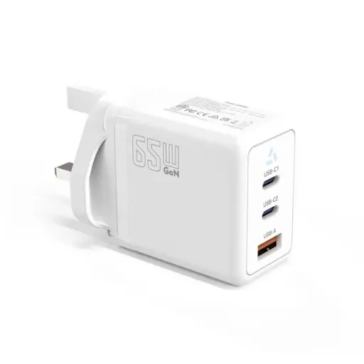 Read More
 -
USB-A vs USB-C Charging: What OEM Buyers Need to Know
June 8, 2026Your customers plug in a USB-A cable they have used for three years, and their new device takes six hours to charge. They switch t Read More
 -
QC3.0 vs QC4.0: What OEM Buyers Need to Know Before Specifying Fast Charging
June 6, 2026When Raj's team at a Bangalore-based smartphone accessories brand specified QC3.0 adapters for their 2024 power bank line, the Read More

Contact Us
Recommended Products
-
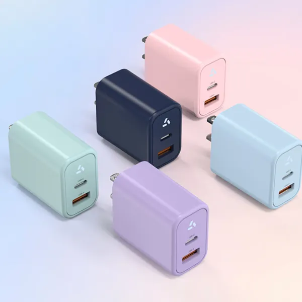
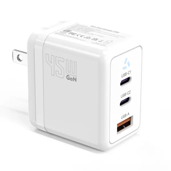
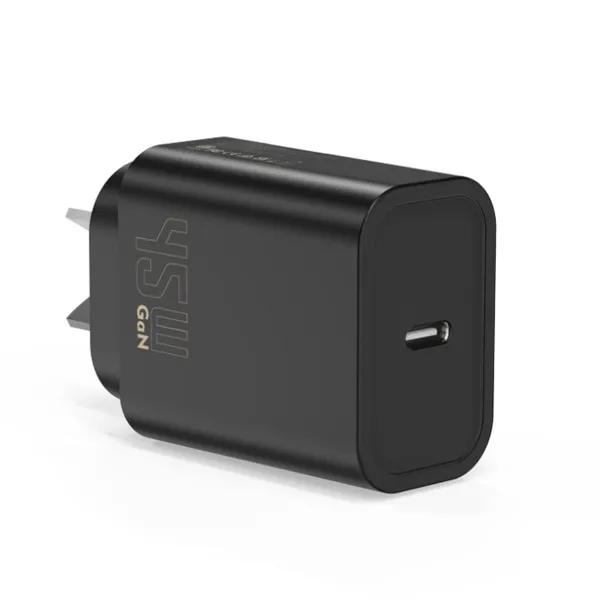
 65W USB-C GaN Wall Charger PD Fast Charging Adapter EU US Plug for Laptop Smartphone and TravelUS$ 6MOQ: 100 Pieces
 -
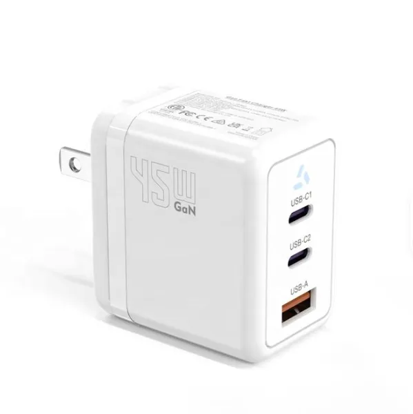
45W GaN USB-C Fast Charger JP Plug PD Wall Charging Adapter for IPhone MacBook and TabletsUS$ 8MOQ: 100 Pieces
-
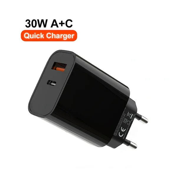
QC3.0 30W USB Fast Charger With 18W Quick Charge Wall Adapter for Android and Mobile DevicesUS$ 4MOQ: 100 Pieces
-
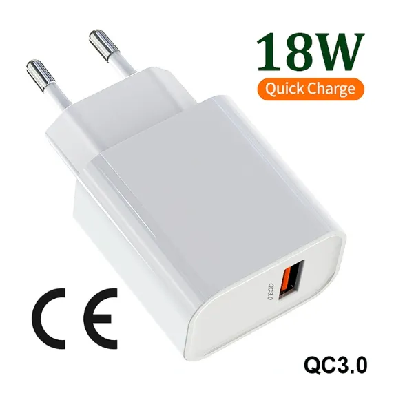
Compact 18W Quick Charge 3.0 USB Charger 30W Fast Charging Adapter EU US Plug for TravelUS$ 2MOQ: 100 Pieces
-
30W USB-C and USB-A PD Fast Charger Compact Wall Adapter for IPhone Samsung and IPadUS$ 3MOQ: 100 Pieces
-
35W Dual USB-C PD Charger Fast Charging Adapter for IPhone Samsung IPad and USB-C DevicesUS$ 3MOQ: 100 Pieces
-
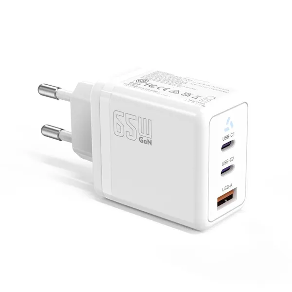
65W USB-C GaN Charger EU Plug Fast Charging Adapter 65W USB-C PD Fast Charge Wall Charger Power Adapter for Macbook ProUS$ 5MOQ: 100 Pieces
-
65W GaN USB-C Fast Charger PD Wall Charging Adapter for Laptop IPhone and Mobile DevicesUS$ 5MOQ: 100 Pieces
-
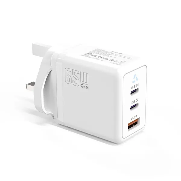
100W GaN USB-C Fast Charger With PD 3.0 for Laptop, MacBook, IPhone & Multi-Device ChargingUS$ 12MOQ: 100 Pieces
-
45W GaN USB-C Fast Charger EU AU PD Fast Wall Charging Adapter for IPhone Tablets With CE REACH PassedUS$ 8MOQ: 100 Pieces
-
QC3.0 65W GaN USB C Super Fast Charger With UKCA 3 Ports PD 3.0 GaN Charger for Iphone Macbook SamsungUS$ 10MOQ: 100 Pieces
-
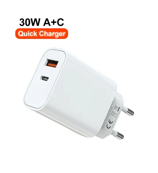
30W USB-C and USB-A GaN QC3.0 Fast Charging Adapter PD Fast Charger Compact Wall Adapter for IPhone Samsung and IPadUS$ 3MOQ: 100 Pieces
-
45W GaN USB-C Fast Charger With Dual Type-C and USB-A Ports PD Wall Charging AdapterUS$ 8MOQ: 100 Pieces
-
Dual USB C Ports QC3.0 30W Fast Charger With EU UK AU US USB-C PD Wall Chargeer 30W PD Power AdapterUS$ 3MOQ: 100 Pieces
-
Compact 65W GaN USB-C Wall Charger With Dual USB-C Ports and USB-A Fast Charging Adapter With CE UKCA ETL SAAUS$ 10MOQ: 100 Pieces
-
QC3.0 Fast Charging Adapter PD30W USB-C USB-A GaN PD Fast Charger PD 3.0 GaN Charger Compact Wall Adapter for IPhone Samsung and IPadUS$ 3MOQ: 100 Pieces
-
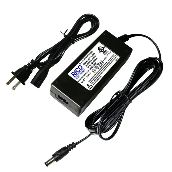
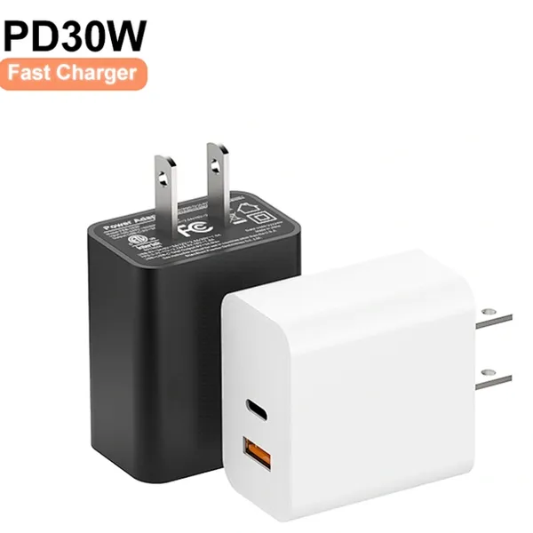
12V 5A 60W US EU AC DC Adapter LED Driver LED SMPS AC to DC Switching Power SupplyUS$ 5 - 7MOQ: 50 Pieces
-
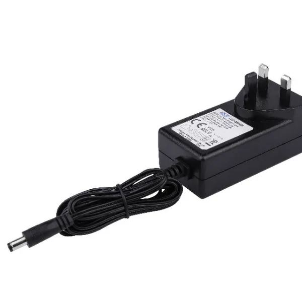
CE FCC CUL SAA KC PSE 24Vdc 48W Switching Power Supply AdaptersUS$ 5 - 7MOQ: 50 Pieces
-
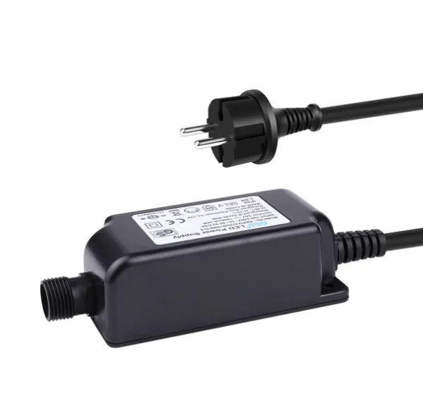
CE GS UKCA SAA CUL Qualified Waterproof Switching Power Supply Ip68 PSE UL SAA GS 12V 2AUS$ 3 - 6MOQ: 50 Pieces
-
12V 1A Factory OEM Waterproof AC Adapter for Laser Light Table Lamp ac dc Adaptor With TUV CE GS for EU MarketUS$ 5 - 7MOQ: 50 Pieces